![]() the Best Wafer Inspection System in the world. . . probably
the Best Wafer Inspection System in the world. . . probably
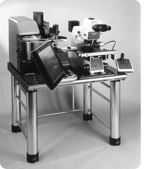
This machine was designed primarily for the inspection of Silicon Wafers.
These wafers are used in the Semiconductor Industry to produce the chips
which are the building blocks of most modern electronic equipment.
The value of each wafer can be hundreds or in some cases even thousands
of pounds, but they can be very easily ruined by faulty handling equipment.
The machine described here has facilities for visually inspecting both sides of the wafers,
and also for the microscopic inspection of the intricate circuitry on each die (chip) on the wafer.
Following there is a collection of pictures and a lot of technical stuff about this machine, which at some point seemed
to involve me in everything from the fundamental Laws of Physics though to the latest software techniques
- and a lot of pretty tricky stuff in between.
* but it was worth it - I think!
From left to right the main features are:
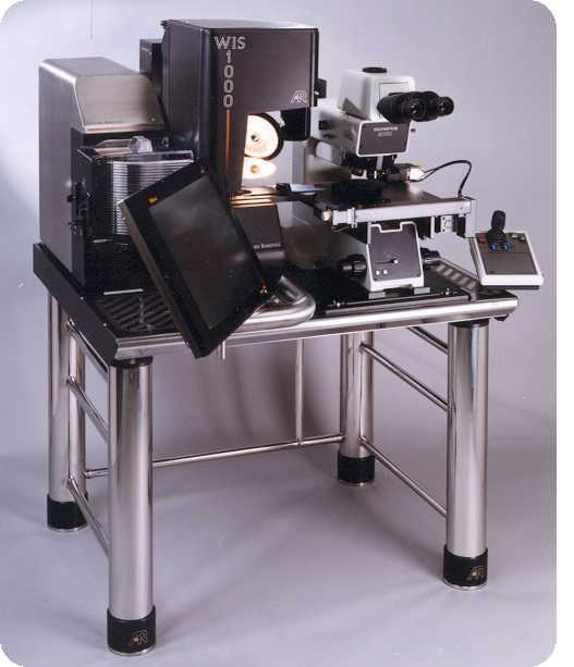
The main control system consists of the CPU and control boards for motor drives, sensor input, vacuum control and a frame grabber that is shared between the OCR system and the video camera.
The joystick is used to tilt and rotate the wafer during the topside inspection and to rotate the gripper mechanism that is used for the rearside inspection.
It also controls the XYtable on the microscope - the motion can be finely controlled such that even under the highest magnification the wafer can appear to be moving very slowly, or by pressing the joystick "boost button" the whole of the wafer surface can be crossed in less than one second.
And finally, the joystick is also used to control the screen cursor for interaction with the GUI as an alternative to the touchscreen.
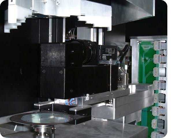
In this picture the inspection cover has been removed and you can see the three-armed gripper mechanism holding a wafer.
The cover itself contains a bright light to illuminate the wafer during the topside inspection,
and a small video camera to view the rearside of the wafer.
The gripper can pivot upwards to present the rearside of the wafer to the operator for initial inspection.
The whole gripper assembly can be raised to position the wafer vertically in front of the video camera which is located inside the inspection cover.
A live image of the wafer can be displayed on the monitor at 4X magnification.
Due to the stepped construction of the gripper jaws, they can hold wafers from 4" to 8" diameter at approximately the same jaw positions.
The aligner is the mechanism which maps the position of the wafer to the machine
- this needs to be done before any of the other inspection processes can occur.
When the wafer is first picked up from the cassette it may be facing in any direction
- also it may not have been placed centrally in the slot and so the position of its exact centre is unknown.
The aligning process is as follows:

Here we see a wafer held by vacuum on the end of the linear arm mechanism.
It is being offerred to the microscope chuck at which point the vacuums will be switched
and the transfer will occur.
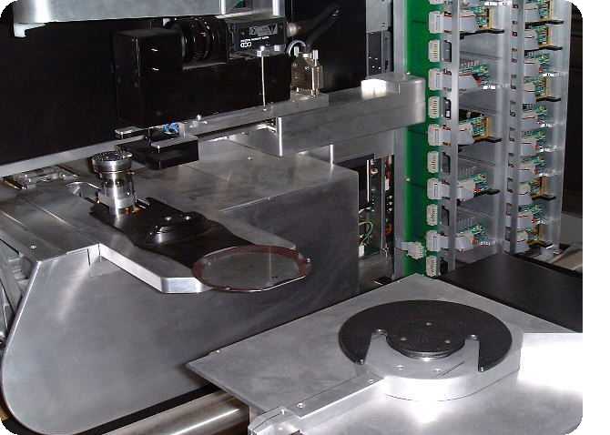
If you are wondering how it can jump the gap from the arm to the chuck, then let me tell you that this is actually a temporary mounting for the microscope chuck and not the real thing. But at least it shows the principle involved - doesn't it??
This is the main PCB that I spent many weeks designing.
It is a 4-layer board with the main tracking layers sandwiched between
a layer for the ground plane and a layer for the power tracks.
The connectivity is extremely complex with approximately 1000 individual channels, many of which
have multiple connections.
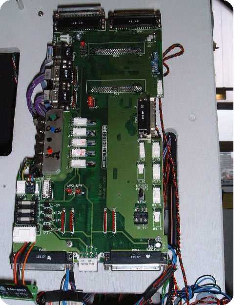
I also designed several other reasonably complex PCBs for various modules in the system, but the interesting aspect of this board is that it contains a link to essentially every part of the system.
It is the common junction through which every signal has to pass at some point, hence my reference to the "spinal column".
The PCB manufacturers told us that this was the most complex board they had ever made. When it arrived I made a point of populating it personally and wiring all of the connectors. I plugged everything in, turned it on, thinking anxiously of the hours of endless checking and painstaking attention to the most trivial details - and it worked perfectly first time!!
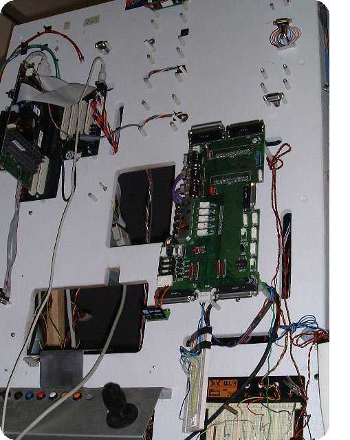
This is the testrig used to develop the system. It was used to mount the control components which
were eventually to be fitted into the machine housing.
Although it may not look the most perfect development environment
it was a great way of keeping everything together and also providing easy access.
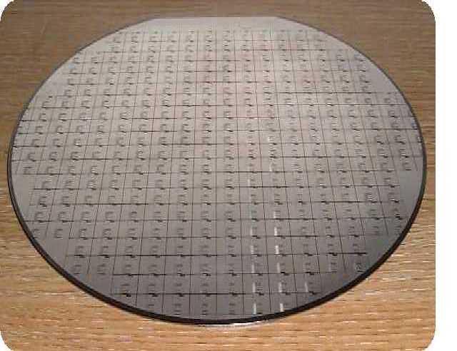
This is an example of a typical wafer to be handled - it is 6 inches diameter (150mm),
and contains almost 300 dies - an average type of wafer.
( The Metric System is widely used in the Semiconductor Industry,
but wafer diameters are commonly quoted in inches! )
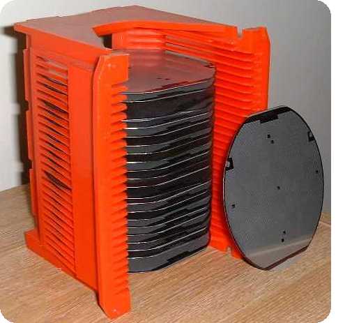
Here is an example of a cassette used to store wafers - this one is for 4 inch (100mm) wafers, and has 25 slots.
